Please see Google Scholar for a complete list of publications and citations.
We are working towards developing new materials for sustainable technological progress in the coming decades. We aim to control and understand materials across a broad range of relevant length scales – including crystal structure, interfaces, surfaces, morphology, and even including local atomic displacements. To do this, we employ state of the art nanocharacterization of materials and devices, combined with highly controlled atomic layer-by-layer growth, to advance the science of functional materials systems and engineering them to design new devices.
Growing Next Generation Ferroelectrics and Multiferroics
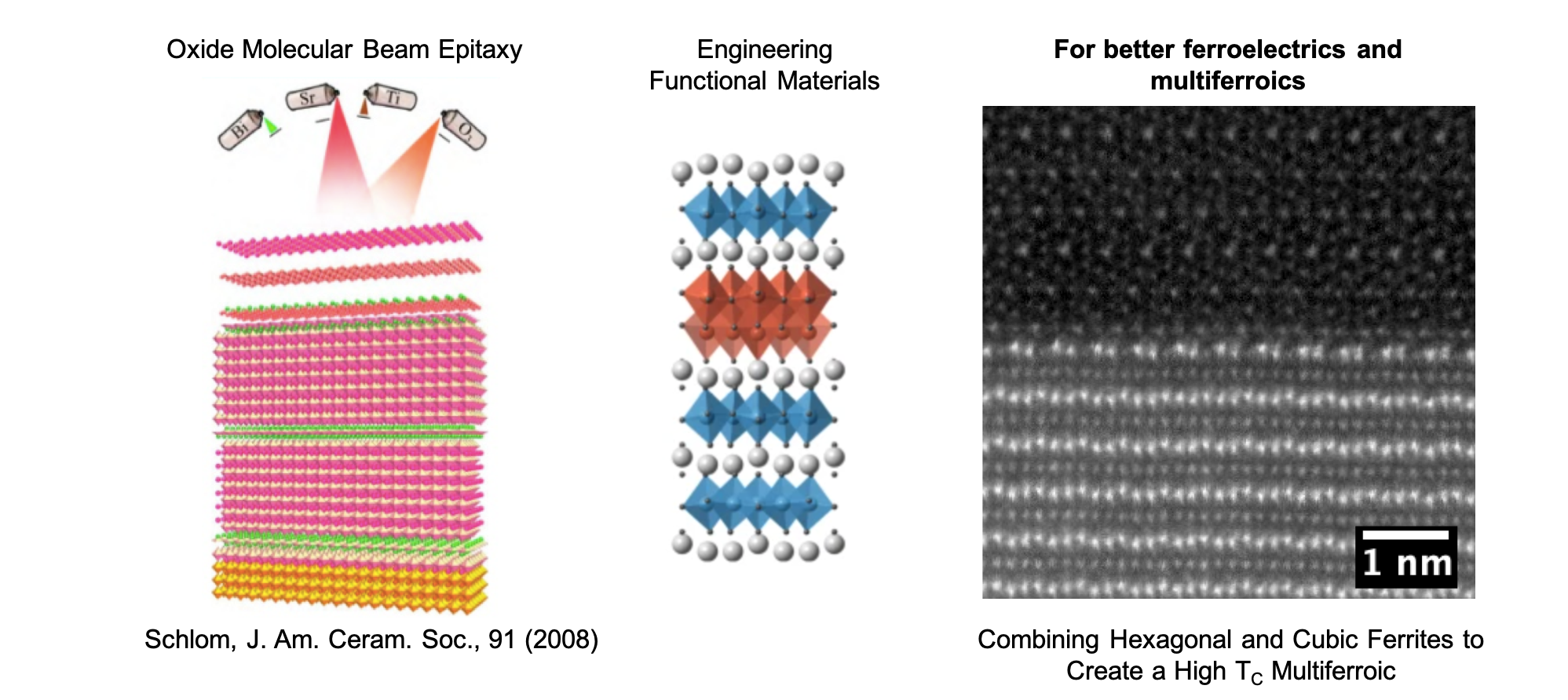
Complex oxides have highly tunable compositions and structures for hosting diverse and record-holding properties in functional materials systems such as ferroelectrics, piezoelectrics, superconductors, and multiferroics. The diversity of properties in this system arises from the interplay between the many degrees of freedom – such as spin, charge, and orbital – as well as several competing potential ground states. One effective way to generate new states in oxide materials is through interface engineering, which locally breaks symmetry and alters the electronic structure. Oxide interfaces, including domain walls, can host emergent phenomena that can dramatically differ from the bulk magnetic, electrical, or optical properties. Additional materials engineering possibilities arise when combining materials into superlattices where interfaces form throughout the “bulk” of the material and inter-layer coupling between interfaces and layers give rise to designer quantum phenomena. Atomically-controlled synthesis methods such as molecular beam epitaxy (MBE) are powerful tools for manipulating and controlling functional and quantum materials. These thin film deposition techniques can epitaxially stabilize metastable crystal structures and symmetries with appropriate choice of substrate, and also create highly controlled, atomically sharp interfaces, superlattices, or surfaces. This sets the stage for synthesizing new materials and interfaces in an ideal, controlled state.
Electron Microscopy as a Toolbox for Understanding Materials
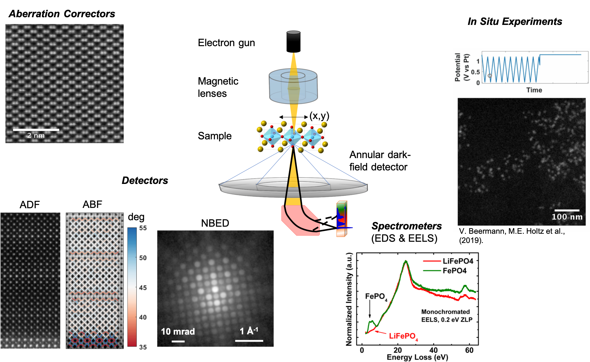
Scanning Transmission Electron Microscopy (STEM) is a powerful toolset for understanding these material systems at atomic and nanometer scale. With techniques such as atomic resolution imaging and spectroscopy STEM-EELS (electron energy-loss spectroscopy) we can investigate spatially varying chemistry with composition mapping and electronic structure measurements. Recent advances in scanning diffraction measurements make it possible to quickly map full diffraction patterns at hundreds of thousands of scan positions in a sample – revealing unprecedented detail in nanoscale strain, crystal structure, and local electric fields. By combining these advanced techniques with in situ measurements, detailed dynamic information of material operation and degradation can further improve our understanding of the material, allowing us to work towards realizing better materials.
Electron Diffraction, Nanometer by Nanometer
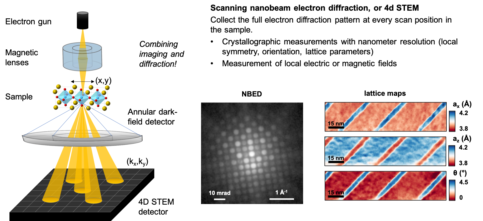
With the advent of fast, pixelated detectors, it is now practical to collect diffraction data at every scan point in an image to generate information-rich four-dimensional data sets (x, y, kx, ky), in a technique called 4D STEM (Fig 3). This enables high-resolution, quantitative mapping of crystal structure, strain, and electric and magnetic fields across large length scales.
Unusual Interface Effects in Dimensionally Confined Improper Ferroelectrics
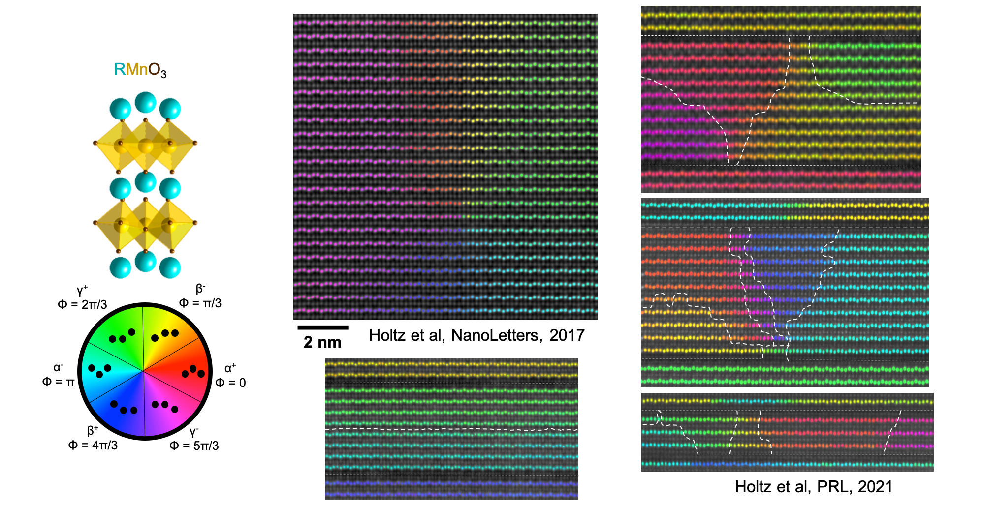
Ferroelectrics and multiferroics are promising candidates for next generation electronic devices, such as memory and storage for computation. However, technical barriers must be overcome for these materials to reach practical applications. For one, low coercive fields are necessary to facilitate fast, low-energy switching, and it is critical for them to maintain the desired functionality in nanoscale device geometries. Magnetoelectric multiferroics have additional challenges in having strong, coupled magnetic and electrical ordering above room temperature.
Interfacial engineering of these materials opens doors to exploring exotic phenomena and driving better materials performance.
Development of Materials for Energy Conversion and Storage
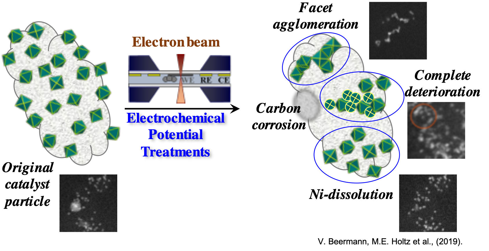
Understanding the degradation and operation of materials for energy conversion and storage is critical for the advancement of the clean energy technologies. Surface and interface effects are critical aspects of materials behavior, and these processes are often heterogeneous on the nanometer scale. Devising experiments – such as the in situ electrochemical experiment above – or by highly controlling material geometries – such as controlled thin film growth – will enable us to tease apart mechanisms on relevant length scales to gain fundamental understanding of these critical materials.